拓扑绝缘体是一种全新的量子物质态,其体电子态是有能隙的绝缘体,而表面则是由于自旋轨道耦合作用产生的由时间反演对称性保护的无能隙表面电子态。我们通过气相化学沉积的方法成功制备了Bi2Te3和不同Se含量掺杂的Bi2Te3的纳米片和纳米线/带,对纳米结构拓扑绝缘体表面态的保护进行了研究。我们报道了成份和栅极电压对化学方法制备的Bi2(Te1-xSex)3纳米带的输运性质的调控。增加Bi2Te3纳米带中Se含量可以有效压制块体载流子输运,在x大于10%时Bi2(Te1-xSex)3纳米带的导电性从金属性转变到半导体性质。在Bi2(Te1-xSex)3纳米带x大于20%时,栅极电压使其电阻(或电导)产生双极化场调制效应,表明从无能隙表面态的贡献的增强。在化学气相沉积的Bi2(Te1-xSex)3的纳米带中发现双极化场效应,说明通过掺杂和控制纳米带的厚度可以有效地降低体态对表面态的影响,对于拓扑绝缘体相关的基础性质和最终应用有着重要意义。相关的工作发表在ACS Nano 7 (2013) 2126,
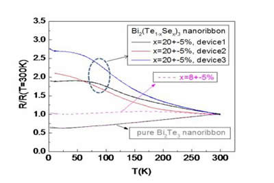
Composition-tuned temperature-dependent transport in Bi2(Te1-xSex)3 nanoribbons. The dependence of resistance on temperature showing the transport property changes from metallic into semiconducting as the concentration of Se increases in Bi2(Te1-xSex)3 nanoribbons.
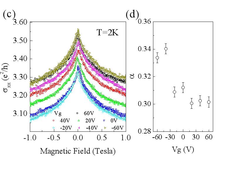
Magneto-conductivity of the device at different gate voltage showing weak antilocalization effect in Bi2(Te1-xSex)3 nanoribbon. The symbols are data and solid lines are fits. (d) The fitting parameter α in the weak antilocalization fit vs. gate voltage. |