Hetero-structures based on 2D materials has been attracted global interests since the first discovery of graphene on hexagonal boron nitride (h-BN). Due to the atomically flat, chemically inert, and dangling-bond free surface of h-BN, graphene is able to manifest super high electronic mobility which surpasses 3-4 orders of magnitudes of that on conventional silicon wafer. It thus promoted the experimental demonstration of fractional quantum Hall effect in this system.
Graphene is known to have zero band gap, and semi metal properties with its conduction and valence bands touching at a point where two Driac cones joint. Together with ultra-high electron mobility, graphene/h-BN heterostructure is predicted to be the very platform for studying electron optics. For example, at the interface of a sharp pn junction, ballistic electrons can incident and get refracted like photons often do obeying the Snell’s law.
The different here is that optical media in nature always show a positive refraction index. However, predicted in 1968 by Veselago et al., light rays can be focused perfectly if they are refracted by a planar lens with negative refraction index. Inspired by the above hypothesis, a electronic version of Veselago lens was demonstrated theoretically in graphene (Fig. 1), where electrons can indeed show focus and defocus on the two sides of a pn junction, by tuning the carrier density on either side of the junction. This is a great example on the application of electron optics, as electron focus and de-focus can physically provides “on” and “off” states, all controlled by gate effect.
Nearly 10 years after the theoretical prediction, experimental demonstration of Veselago lens in graphene is still missing, mainly due to the following technical challenges: 1) electrons has to be fully ballistic in the device; 2) interface of the pn junction has to be sharp enough compared to the electron wavelength. Unfortunately, conventional lithography could not provide such a sharp interface of pn junction. Lead by the Columbia university group, researchers at Georgia University and Institute of Metal Research solved the problem by utilizing mechanically exfoliated graphite as a local gate, which processes atomically flat edge and defines super sharp pn junction interface working together with a remote gate.
The device made by van der Waals hetero-structure of graphene/h-BN with local graphite gate showed, at liquid helium temperature, high signal to noise ratio measurements of negative electron refraction in the paradigm of magnetic focusing under mild magnetic fields. Moreover, the work demonstrated also the possibilities of extracting the parameters such as the junction width and incident angle-dependence of the transmission probability of electrons. The device was ballistic below 70 K temperature, which paves the way for the electron optics and their applications on gate-tunable electron switch using Veselago-type focus.
Our work has been published on Science 353 (2016) 1522. Full text link:http://science.sciencemag.org /content /353/6307/1522)。
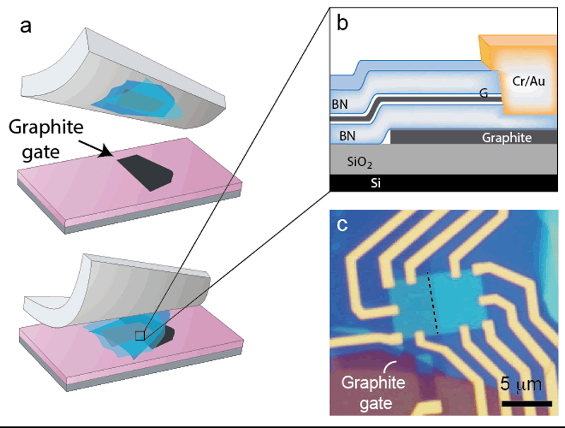
图1. 实验制备的石墨烯-氮化硼异质结构加工示意图和器件光学照片。
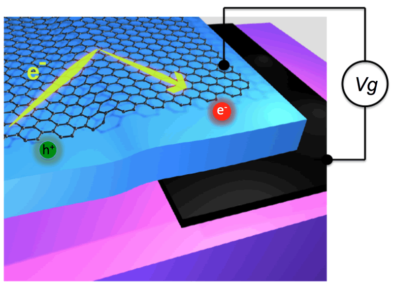
Fig. 1. Schematic picture of electron negative refraction at the interface of the pn junction.
