Optical electrical properties of Bi2Te3/Si PN junctions |
|
|
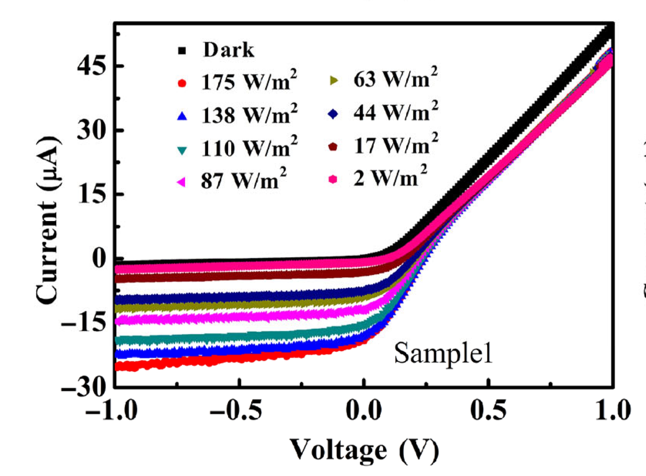
We report on the photovoltaic effects of chemical vapor deposition grown films of n-type topological insulator (TI) Bi2Te on p-type Si substrates. Studying samples with different surface smoothness, we find that films with big size nanoplates and smooth surface on p-Si show good p-n diode characteristics under dark and light illumination, and display good photovoltaic effect under broadband range from ultraviolet (UV), visible to near infrared (NIR) wavelength.Under light illumination of 1000nm wavelength, we obtain the value of ISC =19.2μA and VOC=235mV for the short circuit current and open circuit voltage. The maximum fill factor (FF) increases with decreasing wavelength or light density and reaches 35.6% under 600nm illuminations. The photoresponse of n-Bi2Te3/p-Si device can be effectively switched on and off in millisecond time scale. These findings have implications for both the fundamental understanding and solar cell device applications of TI materials.
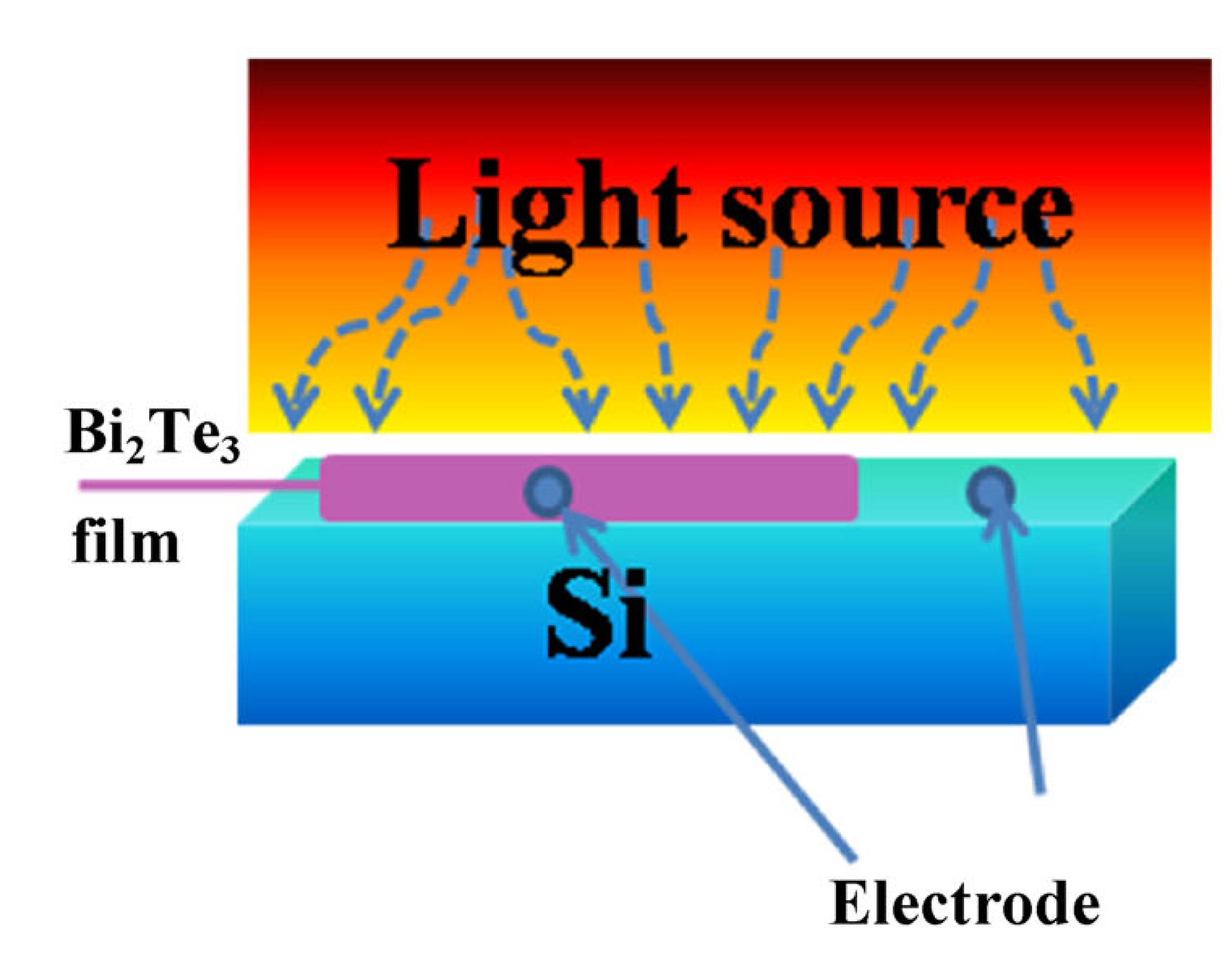
Fig. (a) Schematic of n-Bi2Te3/p-Si junction structurefor measuring photovoltaic effects. (b) The I-V characteristics of junction with different light density under illumination (λ=1000nm). | |