Tunnel contacted MoS2 transistor makes thinnest polarity-tunable rectifier |
|
|
Atomically thin 2D semiconducting materials integrated into van der Waals (vdW) heterostructures have enabled architectures that hold great promise for next generation nanoelectronics. However, applications based on one single 2D material in integrated-circuits (especially as CMOS-type logic devices) are still missing. The demonstration of a bipolar device that is shown to be compatible for both diode and transistor operations is highly desired.
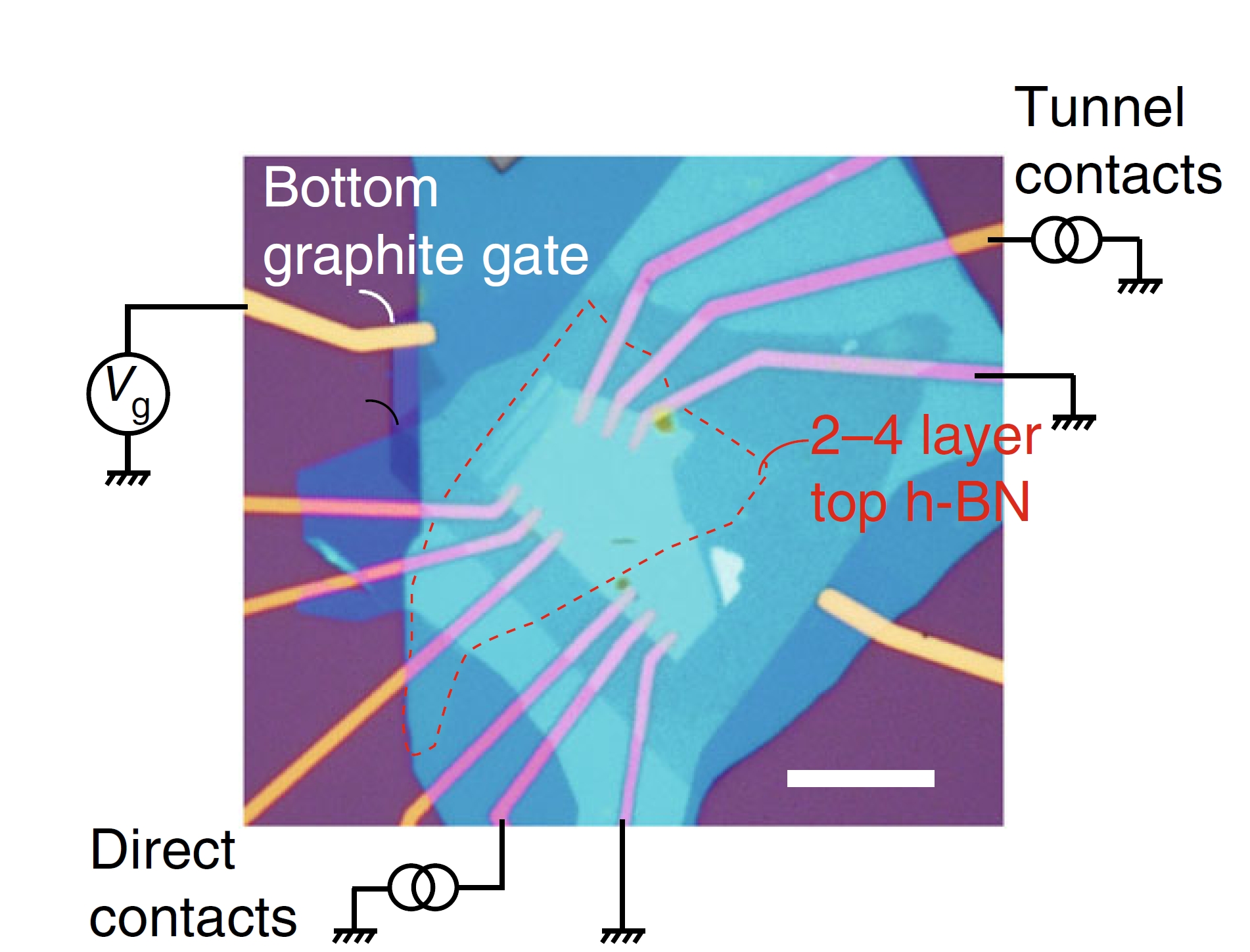
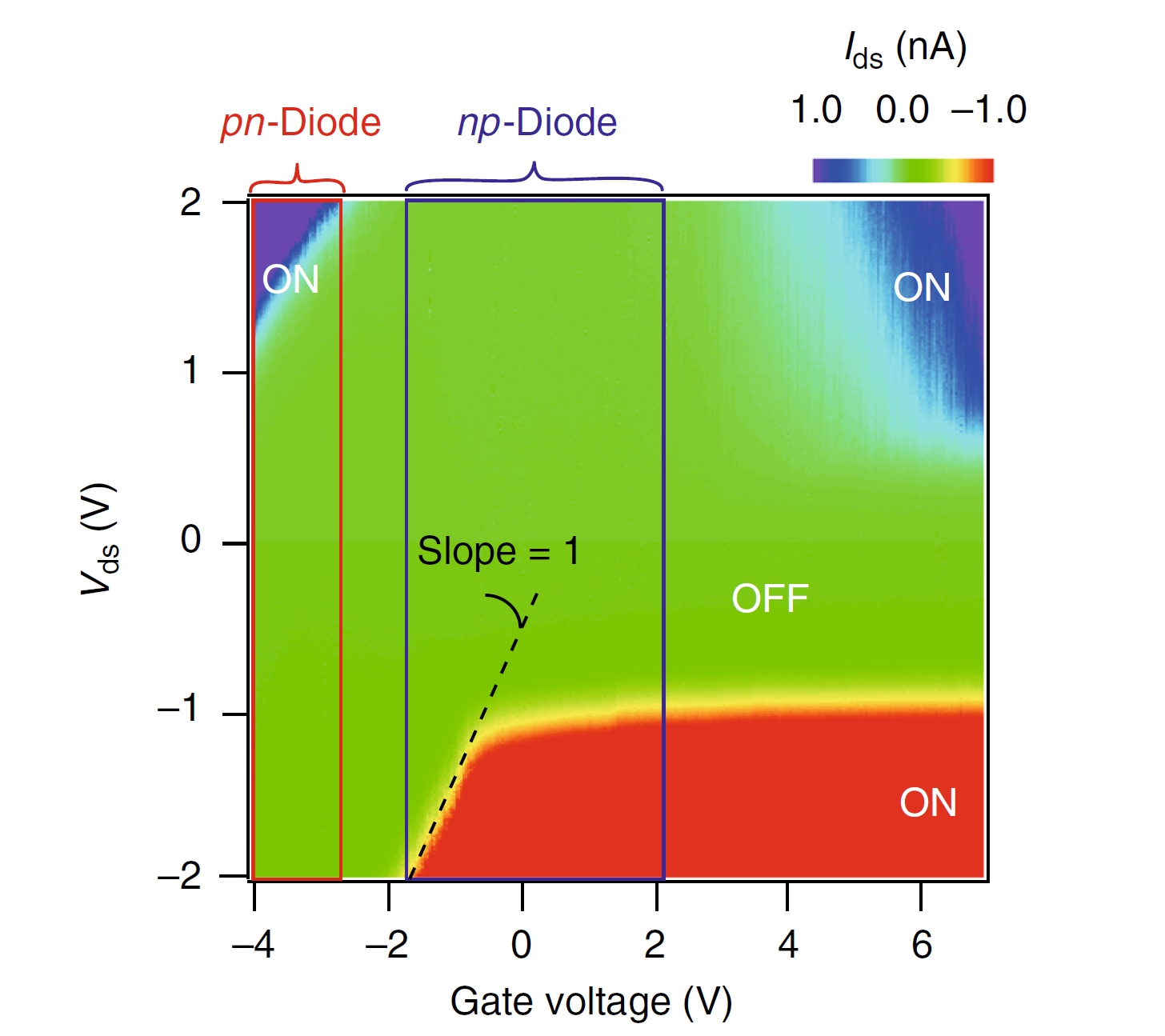
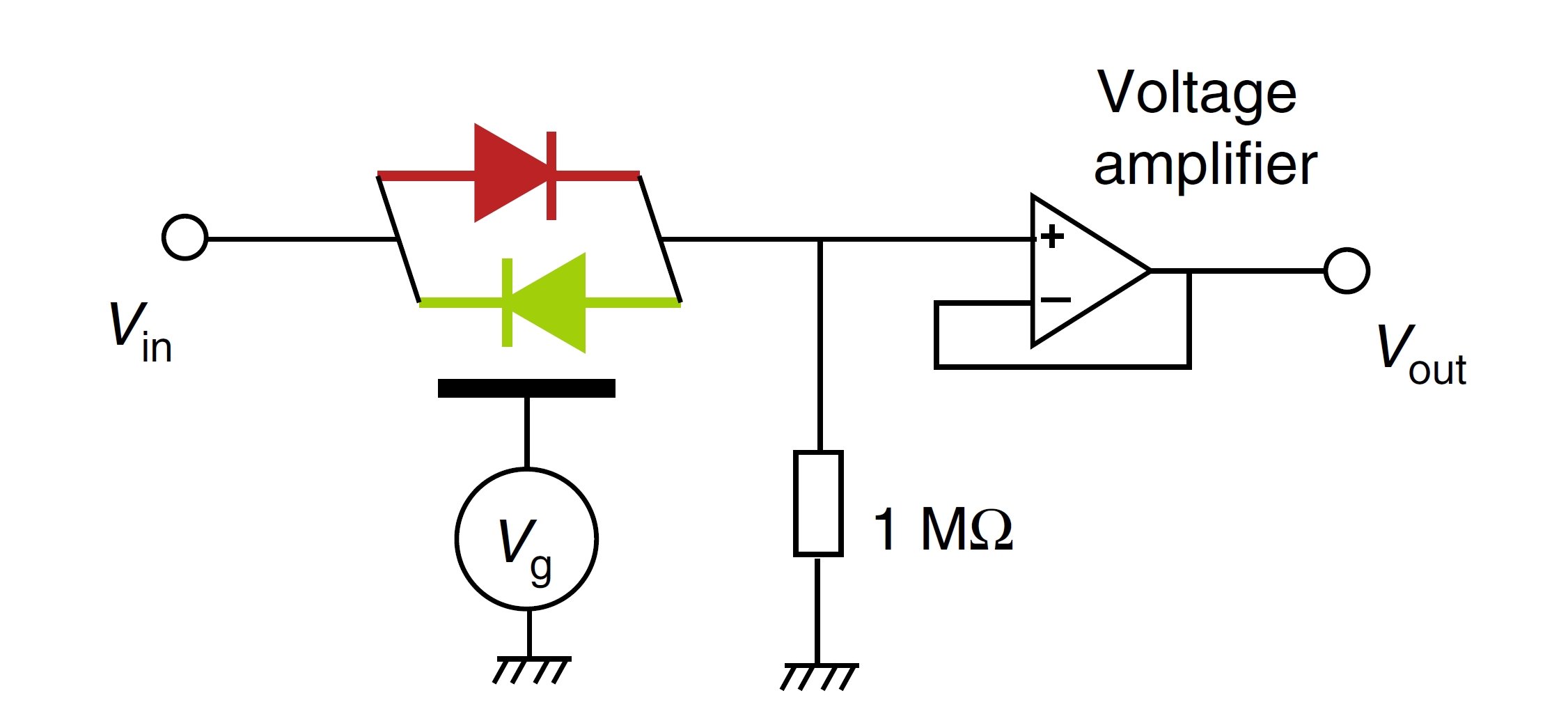
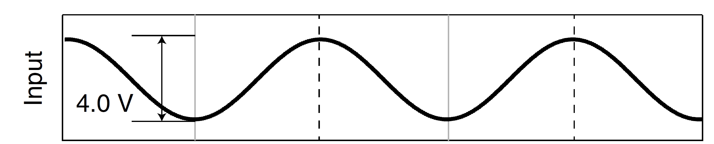
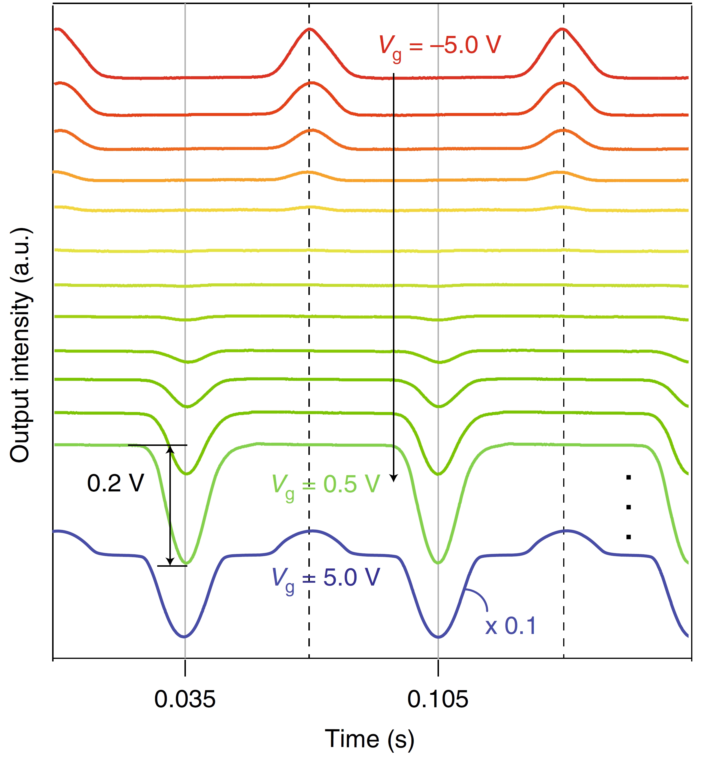
Fig. a) Optical image of the MoS2 TC-FET; b) IV characteristics in the space of gate voltage and source-drain voltage; c) Schematic of the circuit for MoS2 TC-FET rectifier measurement; d) an input of sin wave; e) Gate tuned rectifying behavior of the MoS2 TC-FET. We reported a device fabricated by a “reverted vdW stacking” technique, which enables the integration into vdW heterostructures of atomically thin top layers in an easy and highly reproducible way. When these ultrathin top layers are made of h-BN, this technique enables the integration of high quality and wrinkle-free capping layer that, when electrodes are deposited on top make possible the routine fabrication Tunnel Contacted Field Effect Transistors (TC-FETs). It is shown that tunnel barriers readily suppress Fermi level pinning and Schottky barriers that occur at metal/MoS2 contacts (a common pitfall that hinders the application of 2D semiconductors in CMOS logic). The cancellation of band-bending into MoS2 channel leads to homogeneous gate-control of the channel chemical potential across the band-gap edges. Our work, published in Nature Communications 8 (2017) 970, reports the observation of unprecedented features of an ambipolar pn to np diode, which can be reversibly gate-tuned. This technique can be further applied to a broader range of other atomically thin semiconductors and their hetero-structures. It paves the way for future logic applications and high performance switches based on atomically thin semiconducting channel. | |